OEM Development Board
The Certus MiniOEM development kit allows developers to quickly test and integrate Certus MiniOEM into prototypes. It provides the user with access to all of Certus MiniOEM's interfaces with a number of convenient connection options.
It is an important tool for developing and maintaining a Certus Mini within systems.
- Engineers can quickly test product functionality.
- Engineers can debug local implementations by comparing with the known reference design.
- Engineers can use the development kit to upload the latest firmware onto the Certus Mini OEM .
OEM Development Board Overview
The OEM development board is a configurable PCB that provides developers with easy access to all of the features of the Certus Mini OEM module through a number of different interfaces. The illustration shows an image of the OEM development board.
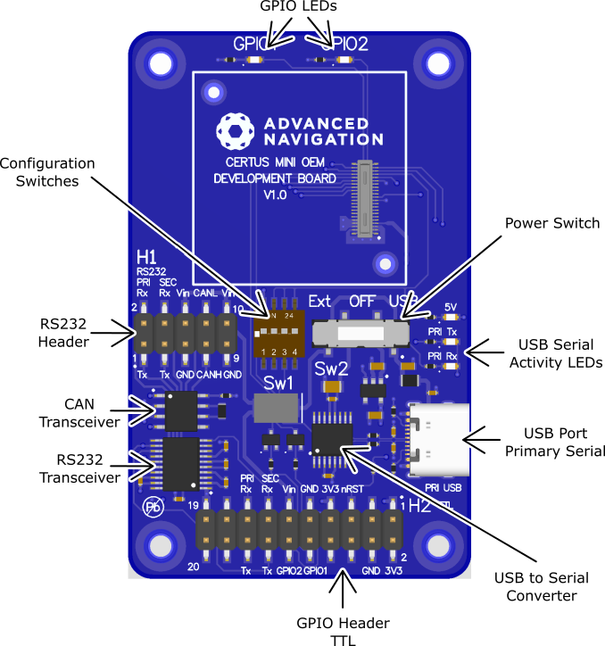
Diagram: Certus MiniOEM Development Board Overview
OEM Power Supply
The power supply is a nominal 5V DC. A high level of power supply filtering has been built into Certus Mini OEM, however it is still recommended that the power supply be low noise (< 20mV peak-to-peak). The unit is only rated for inputs from 4.5 V to 5.5 V, exceeding 6 V can cause permanent damage to the unit.
On start-up of the Certus MiniOEM the device will initially draw an increased impulse current (~400mA for 2 microseconds) whilst it charges on board capacitors. It is important that the user's circuit is tolerant to these small impulses on start-up to avoid unsuccessful power up. It is recommended that a supply is selected that can provide a maximum current of 0.5A. Switch-mode supplies are suitable as Certus MiniOEM has on-board filters to remove any supply noise and ripple.
Serial UART to USB Converter
An FTDI FT232R USB to serial UART converter chip is included on board to allow the Certus MiniOEM to interface directly to a computer through USB. Two status LEDs indicate the flow of data to and from the USB port.
USB drivers for all operating systems can be downloaded directly from FTDI's website at http://www.ftdichip.com/Products/ICs/FT232R.htm.
All development boards are shipped with this interface enabled as standard.
Diagram: USB Serial Converter
Dual RS232 Transceiver
An Exar Corporation SP3222EU dual channel serial UART to RS232 transceiver is included on the development board to allow developers to communicate with the Certus Mini OEM unit via RS232. The SP3222EU allows baud rates of up to 1000000 baud.
Channel 1 of the SP3222EU is for use with the primary serial port on the Certus MiniOEM unit and Channel 2 of the SP3222EU is for use with secondary TX (RS232 TX 2) and secondary RX (RS232 RX 2).
Connection to the RS232 level signals is through a 3x2 2.54mm header, see Illustration 67. This header is on the left of the board and allows developers to attach wires or headers as needed.
Please note that by default the SP3222EU is disabled. Switch 1 turns it on.
![]()
Diagram: RS232 Transceiver
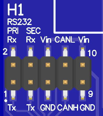
Diagram: RS232 Header with Functions Labeled
CAN Transceiver
The board includes a CAN Transceiver, part #: SN65HVD230Q from Texas Instruments. This part is compatible with the 3V3 logic levels used in Certus Mini and is capable of up to 1MBit/s operation. There is a 120R termination resistor loaded by default between pins 6 and 7.
If the device is being connected to an existing CANbus network, the resistor may need to be removed to ensure proper operation.
![]()
Diagram: CAN Transceiver
GPIO Header and Status LEDs
Users have access to 2 multi-purpose GPIO pins from Certus Mini OEM. These are available on the 7x2 2.54 mm header. Two of these pins (GPIO 1 & 2) are also connected to LEDs on the development board. When using a GPIO in certain input functions, the LED can cause interference with the signal. In this situation, the LED's resistor should be removed. When using the GPIO lines for off board functions it is important to note that these signals are not protected against static charges. (There is tolerance for small over-voltage or over-current events but these should not be relied upon.) Failure to protect the signals may result in damage to Certus Mini OEM. Other pins on the GPIO header include a regulated 3.3V supply from Certus Mini OEM that can supply up to 50mA, the reset line and the external voltage input (VEXT).
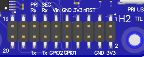
Diagram: GPIO header with functions labeled
RF Connection
Certus Mini OEM variants N and D connect to a GNSS antennas through miniature onboard U.FL connectors A1 (primary) and B2 (secondary). Due to the fragile nature of these connectors, a U.FL to SMA adapter is supplied together with the development board. It is recommended to use this adapter during development to prevent damage to the Certus Mini OEM U.FL connector.
For applications where the development board is placed inside an enclosure it is recommended that developers use a U.FL to SMA cable assembly. These assemblies are available from most of the large electronics distributors.
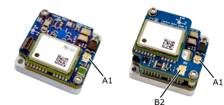
Diagram: Certus MiniN (left) and Certus MiniD (right) GNSS antenna connector locations
Configuration Switches
The OEM development board contains a DIP switch array that allows the user to route signals between the USB to serial converter, RS232 converter and GPIO header. The configuration switches are shown in the illustration below. The default position routes the primary serial port to the USB to serial converter and has secondary TX and RX connected only to the GPIO header. Refer to the table for the switch configuration and functions.
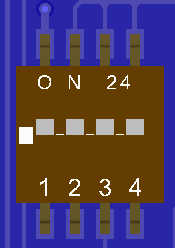
Diagram: Configuration Switches
Note: Only one of switches 2, 3 or 4 should be positioned in the OFF position at one time to avoid short circuits on connected equipment.
| Switch | Default | Function |
|---|---|---|
| 1 | Off (Down) |
Close to enable RS232 Transmitter (Power on RS232 transceiver. When the RS232 transceiver is powered on secondary TX will be connected to RS232 TX2 and secondary RX will be connected to RS232 RX2. The primary serial port TX will also be connected to RS232 TX 1 but the primary serial port RX will only be connected to RS232 RX 1 if switch 2 is turned on.) |
| 2 | Off (Down) | Close to connect primary serial port RX to RS232 transceiver (RS232 RX 1) |
| 3 | On (Up) | Close to connect FTDI RX to RS232 Transceiver |
| 4 | Off (Down) | Close to connect primary serial port RX to GPIO header (UART RX) |
Primary Serial Port to USB
| Switch | Position |
|---|---|
| 1 | Off (Down) |
| 2 | Off (Down) |
| 3 | On (Up) |
| 4 | Off (Down) |
Table: Switch positions for primary serial port to USB (default)
Primary Serial Port to RS232 1 and secondary TX and RX to RS232 2
| Switch | Position |
|---|---|
| 1 | On (Up) |
| 2 | On (Up) |
| 3 | Off (Down) |
| 4 | Off (Down) |
Table: Switch positions for primary serial port to RS232 1 and secondary TX and RX to RS232 2
Primary Serial Port and secondary TX and RX to GPIO Header at TTL levels
| Switch | Position |
|---|---|
| 1 | Off (Down) |
| 2 | Off (Down) |
| 3 | Off (Down) |
| 4 | On (Up) |
Table: Switch positions for primary serial port and secondary TX and RX to GPIO header at TTL levels
Power source
The development board has two power source options; USB power (5V nominal) or an external power source. By default, the development board is configured to use USB power. The external power source can be fed into the board through VExt on either the GPIO header of RS232 header. The external power is a 5 V input.
The power source is selected by a three way switch.
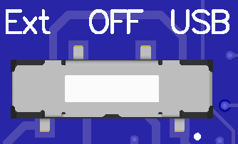
Diagram: Power Switch
| Switch Position | Function |
|---|---|
| Left |
Power switch position for USB power (This doesn't effect the communication of the device.) |
| Middle | Power OFF |
| Right |
Power switch position for external power |
Table: Power switch positions